A look at a electronic component data sheet and setting up a FEA analysis
This particular component is very simple-nothing more than a single transistor-but the analysis techniques are very similar for all. The information we are after are the thermal characteristics shown in figure 2.
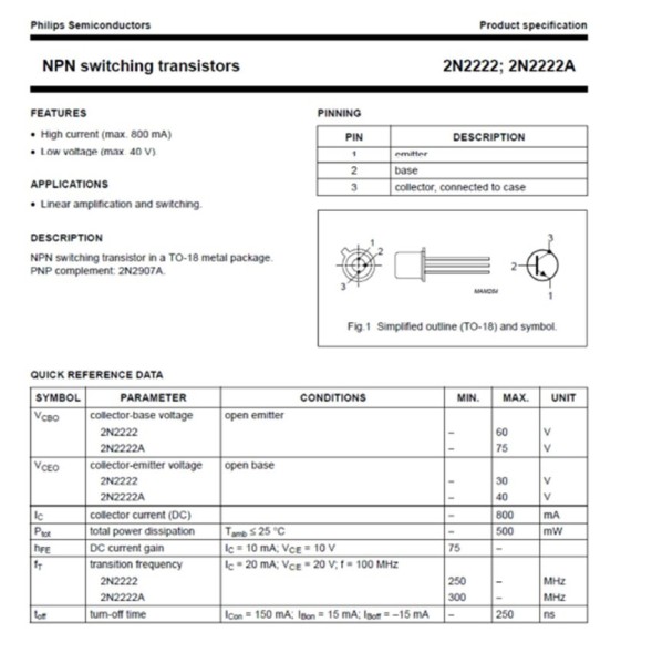
Figure 1 – general information for a transistor
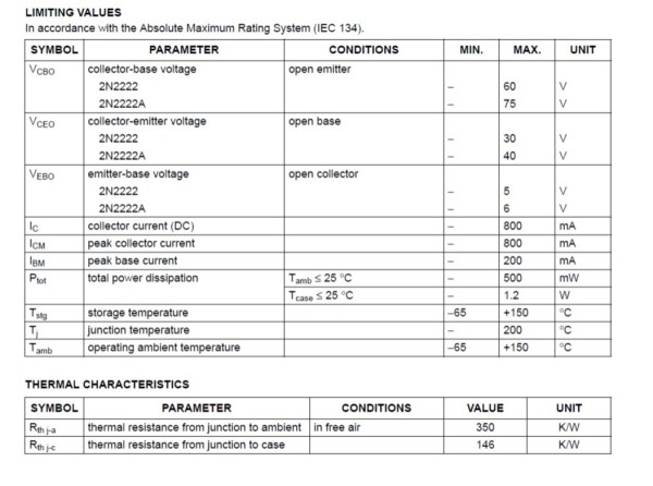
Figure 2 – electrical and thermal characteristics
Key items are junction temperature, ambient temperature limits, and thermal resistance traits. These include theta J-a and theta J-c. Theta J-a is the thermal resistance from junction to air. Theta J-c is the thermal resistance from junction to case. The junction is the electronic part inside the case, which is the packaging around it.
Theta-ja and Theta-jc
Theta J-a and theta J-c are the most common thermal resistances provided. However, some data sheets may not list thermal resistance values. In those cases, calling the manufacturer may help.
The thermal resistance area can be confusing. It’s tough to use these values in a finite element analysis (FEA) model. To predict junction temperature, we need to know the method used to measure it. Many in the industry think theta J-a and theta J-c are good tools for predicting junction temperatures. But, most data sheets don’t specify how researchers measured these thermal resistances. Were they mounted on a board? If so, what are the board’s characteristics, like the number of layers or copper content? Did someone connect the power leads only to the component while you suspended it in the air? To trust these figures, we need to understand how someone generated them.
Junction to Case Method
Junction-to-case thermal resistance shows how temperature drops from the junction to the component’s outer case when it dissipates one watt. For more details, see Mil-STD-883G, Method 1012.1.
To define a simplified model, start by analyzing the component’s volume alone. The goal is to find thermal conductivity. This will help in a systems model that includes the circuit card and housing.
Setting up a FEA Analysis
The figure below shows an example where the volume data came from SolidWorks. The manufacturer provided a junction-to-case thermal resistance of 20 C/W.
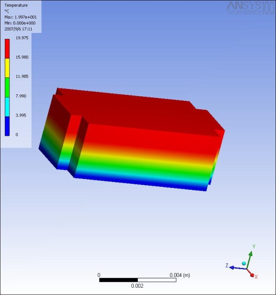
Figure 3: Sample of Junction to Case Solid Model Method
First, take a model of the component volume. Input 1 watt for volumetric heat generation. Set one side of the case to 0 °C. Then, solve for temperatures in the volume. Adjust the thermal conductivity until the greatest temperature equals the junction-to-case thermal resistance. In this example, the greatest temperature should be 20 °C, as shown in the figure above.
To use this single-volume model in a full ANSYS setup, attach it to a circuit board. Input the actual component power into the volume. The resulting greatest temperature gives an estimate of the actual maximum junction temperature.
This method isn’t exact, and many objections may arise. It simplifies how heat flows through the component. The junction-to-case thermal resistance shows this.
Junction to air method
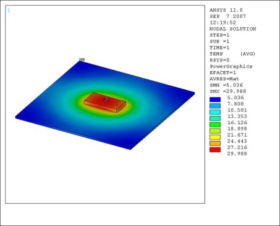
Figure 4 – Junction to air method
This case is not as simple as the junction to case temperature. We want to find the “equal” thermal conductivity for the component volume. This will help us see the correct temperature drop (the junction to air value) when we input 1 Watt.
A component on a low-conductivity PCB measures the junction-to-air thermal resistance. Some heat flows into the board, and some escapes the component surfaces by convection.
Setting Up the Analysis
Start by estimating a natural convection coefficient. Use 5.7 W/(m²-C) for this. Consider adding 4-5 W/(m²-C) for radiation to the surrounding area or use a radiation boundary condition. You need a circuit board size. The JEDEC spec 51-3 states that low effective thermal conductivity test boards should be about 0.09 by 0.09 meters. Next, enter the board thermal conductivity, often called a “1S” board. Based on the JEDEC spec 51-3 and estimating the copper extent at 20% (2 oz copper), we can estimate the board’s thermal conductivity at 3.65 W/(m-C).
Calculate Thermal Conductivity
The component attaches to the board without contact resistance. Set the air temperature to zero degrees C. Use a suitable still air convection coefficient with this model. Change the model’s thermal conductivity. Do this until the highest temperature of the component volume matches the thermal resistance from the junction to the air.
Once you find the correct thermal conductivity, use the component volume as you would use the junction to case volume. Glue the volume to the PCB, apply real power to the component, and set the actual convection and radiation boundary conditions. Solve for the greatest temperature. This temperature estimates the actual junction temperature of the structure.
3D models
Improved modeling techniques for electronic components and circuit cards can enhance estimates. Using a 3D model of the circuit card, with copper traces in every layer, would boost accuracy. Yet, this would create a large analytical model to solve. Copper traces are thin, fine, and many, leading to a very fine mesh. Estimating the copper content in each layer helps predict thermal conductivity. Also, consider the circuit card material’s resistance for a clearer forecast. This method may be less accurate but is easier to use.
Modeling the Junction
You could model the component with a small block or surface inside to represent the junction. This block would generate heat at the junction and dissipate it into the case. Heat would then conduct from the case into the circuit card and surrounding air.
Additional Details
Many improvements could complicate the component model further. Modeling the electrical leads separately gives better insight into the solder and internal wire traces. Yet, this could make the model large and cumbersome, taking a lot of time and money to solve. Also, think about providing this detail for many components—say 20, 30, or 40. Even in a simple case, you must include external dimension models that shape the component and leads. Also, add the thermal resistances.
Component Power
Another critical factor is the power supplied to the component. In most analyses I’ve conducted, I have never received this information with accuracy. You must model the circuit card assembly in circuit card analysis software to get accurate data. Otherwise, to measure current on a completed assembly, you would need to cut the traces. We will discuss other workarounds for this lack of information later.
Norman T. Neher, P.E.
Analytical Engineering Services, Inc.
Elko New Market, MN
www.aesmn.org